
Enhancing Semiconductor Thermoelectrics with Thickness Doping
Advancing Thermoelectric Technology with Innovative Synthesis Methods
Thermoelectricity offers a promising pathway for converting heat directly into electricity and vice versa. This technology holds great potential for harvesting low-grade heat and providing solid-state cooling, which is essential for the development of sustainable electronics. The traditional synthesis of bulk Bi₂Te₃ polycrystalline materials involves complex processes such as melting, ball milling, hot pressing, and spark plasma sintering. These methods aim to introduce various structural defects that enhance the material’s performance.
However, when it comes to creating thin films, the process faces significant challenges. The physical thickness and compatibility with substrates limit the techniques available for deposition. Enhancing the performance of these thin films often relies heavily on post-deposition annealing treatments. Despite efforts such as dopant manipulation in physical vapor deposition or the use of nanobinders in screen-printed processes, achieving a power factor exceeding 20 μW cm⁻¹K⁻² at room temperature in n-type Bi₂Te₃ thin films through single-step synthesis remains a challenge. Additionally, while high-performance thermoelectric films can be obtained by exfoliating from single crystals, their limited scalability (less than 5 cm²) restricts their practical applications.
Conventional methods also struggle with fine-tuning critical parameters like the Seebeck coefficient, electrical conductivity, and scalability in n-type Bi₂Te₃ thin films. Therefore, advanced fabrication methodologies must address three key areas: (1) optimizing carrier concentration and weighted mobility to maximize the power factor; (2) maintaining a high power factor and figure of merit while ensuring superior flexibility; and (3) achieving scalable and cost-effective manufacturing.
In a recent study published in Science Advances, researchers introduced a novel approach that leverages the synergy between magnetron sputtering (MS) and vacuum thermal evaporation (VTE), two widely used techniques in semiconductor industries. This method allows for the deposition of VTE@t%MS-Bi₂Te₂.85Se₀.₁₅ films with precisely adjusted MS-layer proportions. The variable thickness across hetero-depositions contributes to the homo-fusion of semiconductor films with engineered electron and phonon transport.
The modulation of carrier and mobility through variable thickness proportions (t%) via homo-layer fusion is analogous to element doping in materials. Interestingly, the developed VTE@MS-BTS synergistically modulates the Seebeck coefficient, electrical conductivity, thermal conductivity, and mechanical flexibility of the film. As a result, an ultrahigh power factor of up to 30.0 μW cm⁻¹K⁻² at room temperature was achieved in a scalable film measuring 120 cm². The bendability of the film was also enhanced due to induced microstructural defects.
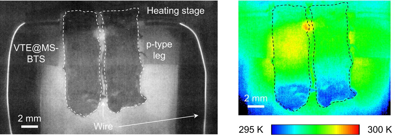
Integrating this advanced film into planar device configurations demonstrated a high output performance for competitive power generation and cooling. According to Dr. Mao, these results provide a pivotal framework for understanding and manipulating structure-property relations in thermoelectric films. They also contribute to the advancement of scalable and flexible inorganic semiconductors.
This research is part of Science X Dialog, where researchers can report findings from their published research articles. For more information about Science X Dialog and how to participate, visit the dedicated page.
More information: Dasha Mao et al, Homo-layer flexible Bi₂Te₃-based films with high thermoelectric performance, Science Advances (2025). DOI: 10.1126/sciadv.adz1019
This study was led by Dr. Yi Zhou from the National University of Singapore and Prof. Jiaqing He from the Southern University of Science and Technology.
Posting Komentar untuk "Enhancing Semiconductor Thermoelectrics with Thickness Doping"
Posting Komentar