
Sum-Frequency Microscope Reveals Invisible 2D Material
Researchers from the Physical Chemistry and Theory departments at the Fritz Haber Institute have discovered a groundbreaking technique to visualize layers of boron nitride that are just one atom thick. This material is typically difficult to observe under optical microscopes because it lacks optical resonances.
To address this challenge, the team employed nonlinear microscopy using infrared light, which causes the material to emit a strong signal and reveals its crystal orientation. This innovation has significant implications for the growing field of designing new (opto-)electronic devices by stacking 2D materials.
The research was published in the journal Advanced Materials.
Why Study 2D Materials?
Two-dimensional (2D) materials are crystalline substances composed of a single layer of atoms, exhibiting unique properties due to their extreme thinness. Although scientists have known about layered materials for over a century, it wasn't until 2004 that the first 2D material, graphene, was successfully produced.
Since then, numerous new 2D materials have been developed, leading to innovative applications. These thin layers are highly sought after for use in future technologies, including electronics, energy systems, and optical components. As a result, they are the focus of extensive research.
The Challenge with Hexagonal Boron Nitride
Boron nitride (BN), often referred to as "white graphene," is a layered material made up of boron and nitrogen. It can exist in various forms, such as hexagonal boron nitride (hBN). Like graphene, hBN has a hexagonal lattice structure and is widely used in applications like quantum optics or infrared nanophotonics, or as a substrate or encapsulating material.
For these applications, precise characterization of hBN layers is essential. However, monolayer hBN is transparent across the near-infrared and visible spectrum, making it difficult to study with conventional optical microscopes. This limitation has hindered its use in developing new materials.
For example, identifying distortions and grain boundaries in 2D layers requires accurate mapping. Researchers also stack monolayers of 2D materials to create "van der Waals structures" that can display new and exciting properties. Ideally, this layering could be observed live under a microscope, with the orientation of each layer visualized. Developing such capabilities for hBN is therefore highly desired.
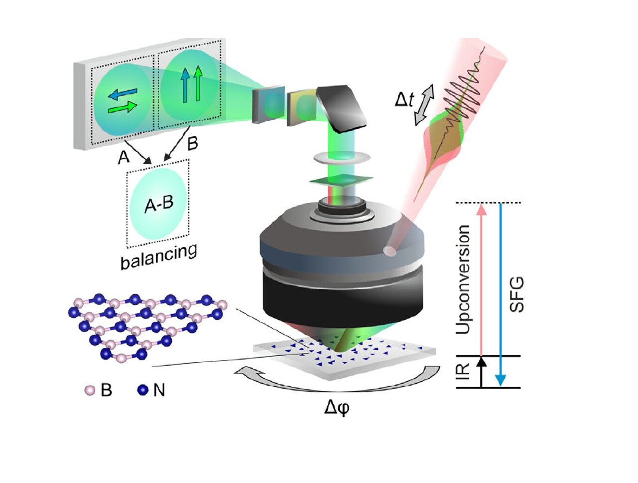
The Sum-Frequency Microscope
The research team at the Fritz Haber Institute overcame this challenge by developing a microscope that uses a trick in nonlinear optics to make hBN visible. Their method, called "phase-resolved sum-frequency microscopy," mixes two laser beams—one in the mid-infrared and one in the visible range—to generate a sum-frequency signal in the sample that is measured.
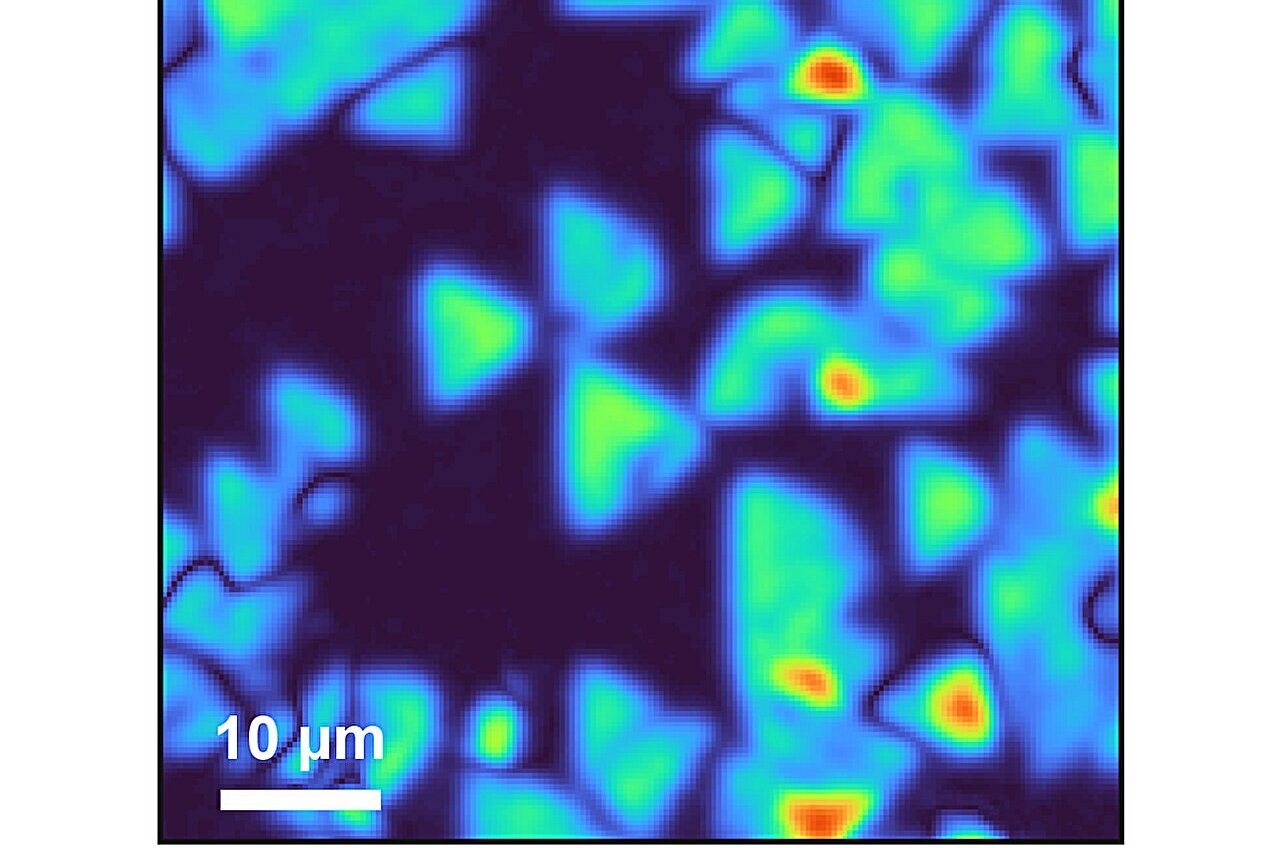
By resonantly driving an hBN lattice vibration, the measured sum-frequency signal becomes very intense, allowing researchers to image large 100 × 100 μm² sample areas in less than 1 second. They can even visualize the crystal orientation.
Thanks to their new microscope, the researchers found that the 2D layers of hBN that grow in triangular domains display nitrogen-terminated zigzag edges. Additionally, the observed high nonlinearity in the vibrational resonance frequency highlights monolayer hBN as a promising material for frequency upconversion—from the infrared into the visible—in new optoelectronic devices.
Fruitful Cooperation of Two FHI Departments and International Partners
This study exemplifies the collaborative research philosophy of the Fritz Haber Institute, combining the expertise of multiple research groups from different departments and international partners to tackle major scientific challenges. The hBN monolayer samples were synthesized at Vanderbilt University and analyzed using sum-frequency microscopy at the Physical Chemistry Department at the Fritz Haber Institute.
To support advanced characterization of the samples, atomic force microscopy (AFM) images were recorded by collaboration partners in the Department of Physics at Freie Universitat Berlin. Finally, the expertise of the Theory Department at the Fritz Haber Institute enabled the extraction of crystallographic details.
Prospects of the New Experimental Method
The newly developed microscope offers clear advantages over existing methods. First, it makes optically transparent materials visible in an optical microscope. The resulting images have much higher contrast than traditional AFM images, and the use of vibrational resonance enhancement enables "live imaging" of hBN, including online information on its crystal orientation. These advanced capabilities make controlled fabrication of layered van der Waals structures feasible in future applications.
Finally, the authors anticipate extending this new imaging tool as a noninvasive and label-free method to study a wider range of stacked 2D materials, as well as their combinations with anisotropic molecular assemblies.
More information:
Niclas S. Mueller et al, Full Crystallographic Imaging of Hexagonal Boron Nitride Monolayers with Phonon-Enhanced Sum-Frequency Microscopy, Advanced Materials (2025). DOI: 10.1002/adma.202510124
Posting Komentar untuk "Sum-Frequency Microscope Reveals Invisible 2D Material"
Posting Komentar